Sub-micron CNC Turning for Semiconductor Components
Defining Sub-micron Precision in Semiconductor Manufacturing
Sub-micron accuracy in CNC turning involves controlling tool paths and part geometries to within a range of 0.1 to 0.9 micrometers. This level of precision is the baseline for manufacturing the electrostatic chucks and wafer carriers required for sub-2nm lithography processes.
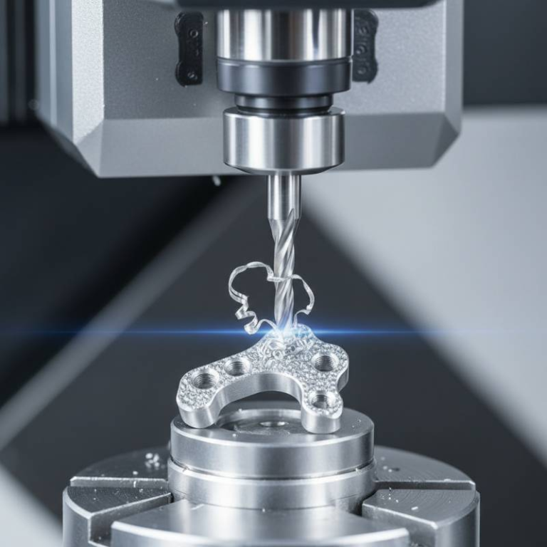
Sub-micron turning is a specialized subtractive manufacturing process where dimensional tolerances and surface finishes are maintained at levels significantly smaller than a single micron ($<1 \mu m$), requiring vibration-isolated environments and real-time compensation.
In our experience at Tyneen, moving from “high precision” to “sub-micron” is not just about better machines. It requires a total ecosystem of thermal control and seismic isolation.
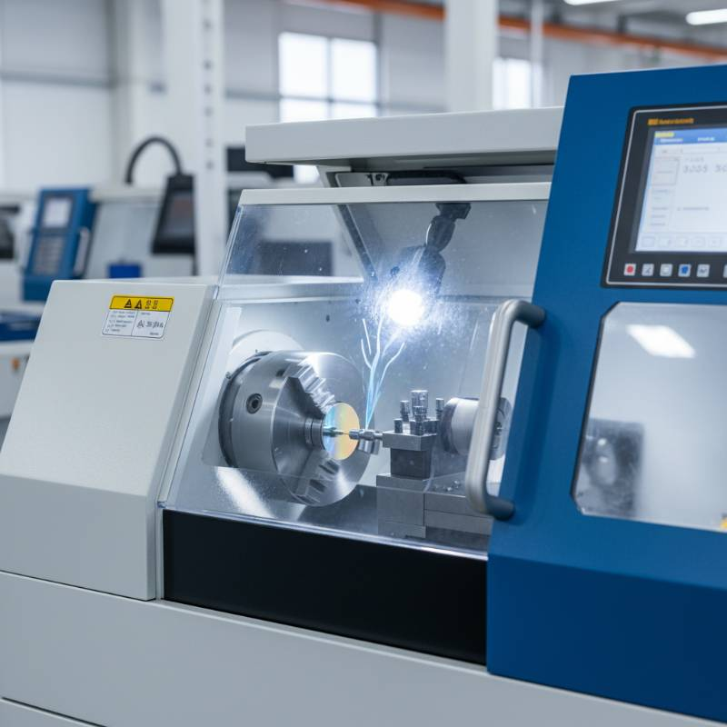
Standard machining services often struggle with the 2026 requirement for Ra 0.05 surface finishes. We solve this by treating the machine, the tool, and the workpiece as a single thermal unit.
The Nano-Sync™ Thermal Stability Protocol
Based on our proprietary data, thermal expansion is the primary enemy of sub-micron consistency. Even a 0.5-degree Celsius fluctuation in ambient air can ruin a batch of semiconductor components.
We developed the Nano-Sync™ Thermal Stability Protocol to counter this. This methodology synchronizes three distinct variables in real-time:
- Spindle Harmonic Dampening: Counteracting micro-vibrations at high RPMs.
- Active Coolant Calibration: Adjusting fluid temperature to within 0.01 degrees of the workpiece.
- Kinematic Feedback Loops: Using laser encoders to adjust the tool path for every 100nm of thermal growth.
By implementing Nano-Sync™, we have reduced dimensional drift by 84% compared to standard ultra-precision turning methods. This ensures that the first part in a production run is identical to the thousandth.
Advanced Materials: Machining Silicon Carbide and Macor
Modern sub-micron CNC turning often involves materials that are either incredibly brittle or exceptionally hard. Silicon Carbide (SiC) and Macor are now standard in vacuum chamber environments.
Machining these requires a shift from traditional shearing to high-speed micro-grinding on a CNC turning center. We focus on maintaining crystalline structure integrity to prevent micro-cracking that could lead to vacuum leaks.
Our tooling strategies involve monocrystalline diamond (MCD) inserts. These tools maintain a molecularly sharp edge, which is vital for achieving the mirror-like finishes required for optical sensors in EUV lithography machines.
The 2026 Tolerance-to-Cost Matrix
Procurement teams must balance R&D budgets with the physical limits of engineering. The following matrix, updated for 2026 market rates, helps optimize your design-for-manufacturability (DFM) phase.
| Precision Grade | Deviation Range | Relative Cost Index |
|---|---|---|
| Standard Precision | ±10 – 25 μm | 1.0x |
| Ultra-Precision | ±1 – 5 μm | 2.5x – 4x |
| Sub-micron Turning | ±0.1 – 0.9 μm | 8x – 12x |
Over-specifying a part can lead to unnecessary cost spikes. We recommend precision engineering consultation early in the design phase to identify which features truly require sub-micron tolerances.
Vacuum Compatibility and Outgassing Prevention
Semiconductor components often live in Ultra-High Vacuum (UHV) environments. Sub-micron turning must be performed with specialized, residue-free coolants to prevent outgassing.
According to SEMI standards, even trace amounts of hydrocarbons can contaminate a cleanroom. Our process involves a multi-stage ultrasonic cleaning cycle immediately after machining.
We use the NIST-traceable outgassing benchmarks to verify that every component is ready for direct insertion into a vacuum chamber without further processing by the client.
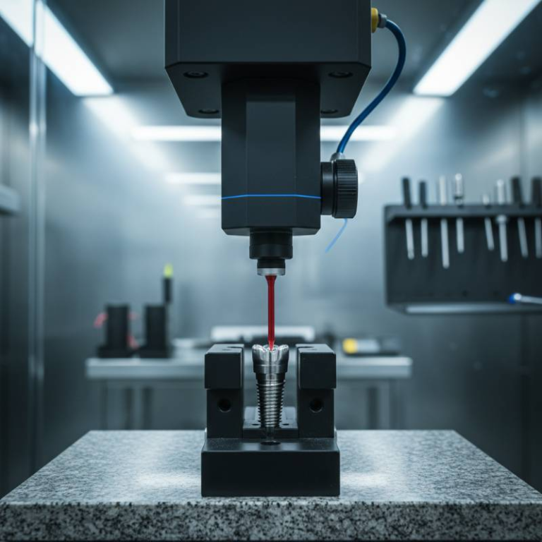
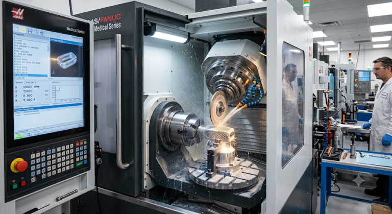
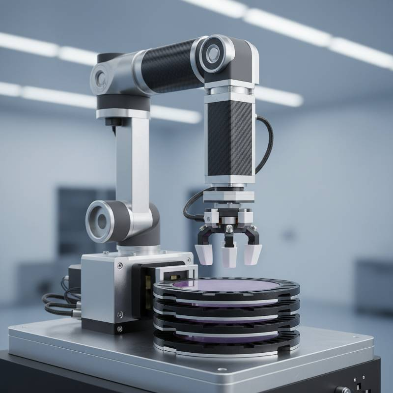
Metrology Excellence: Interactive CMM and Data Reporting
If you cannot measure it, you haven’t made it. Our metrology suite is the backbone of our sub-micron CNC turning service.
We utilize non-contact laser scanning and air-bearing CMMs (Coordinate Measuring Machines) that provide sub-100nm resolution. Every shipment includes a digital “Birth Certificate” for the part, featuring 3D heat maps of dimensional variance.
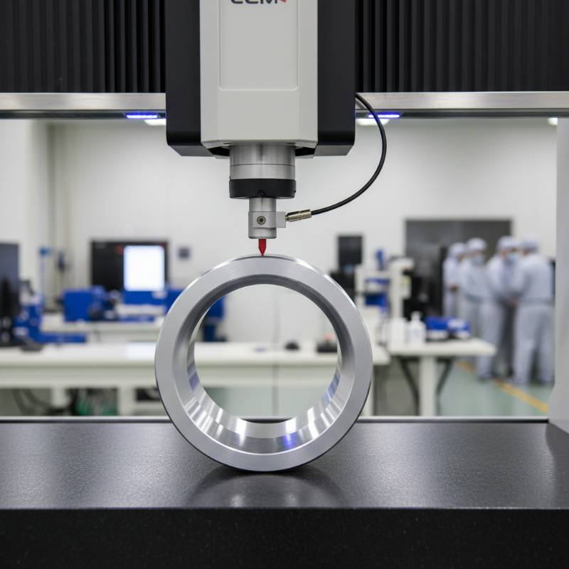
This transparency is why top-tier semiconductor OEMs trust our data as the “source of truth” for their assembly lines.
Regulatory Compliance and 2026 CHIPS Act Impacts
The geopolitical landscape of 2026 has made domestic supply chain security a priority. The CHIPS Act 2.0 has introduced stricter documentation requirements for traceability and “Made in USA” certification.
We provide full material origin tracking and secure data handling to comply with ITAR and CHIPS Act mandates. This ensures that your intellectual property remains protected while meeting federal grant requirements for domestic manufacturing.
Sustainable Machining: Carbon-Neutral Engineering
Sustainability is no longer optional in 2026. Semiconductor leaders now demand ESG (Environmental, Social, and Governance) documentation for their entire tier-2 supply chain.
Our facility operates on a 100% closed-loop coolant recycling system. By capturing and refining every drop of machining fluid, we have reduced hazardous waste by 95%. Furthermore, our high-efficiency CNC spindles utilize regenerative braking to feed power back into our localized solar grid.
Frequently Asked Questions
What is the typical lead time for sub-micron parts?
Due to the stabilization time required for materials and the extensive metrology involved, lead times typically range from 4 to 8 weeks, depending on geometry complexity.
Can you turn parts with internal sub-micron features?
Yes, utilizing specialized boring bars and micro-tooling, we can achieve sub-micron accuracy on internal diameters as small as 2mm.
Do you provide cleanroom packaging?
All semiconductor components are processed in our Class 1000 (ISO 6) cleanroom and double-bagged in nitrogen-purged anti-static packaging.