5-Axis CNC Milling for Semiconductor Process Chambers
Defining High-Precision Milling for the Semiconductor Industry
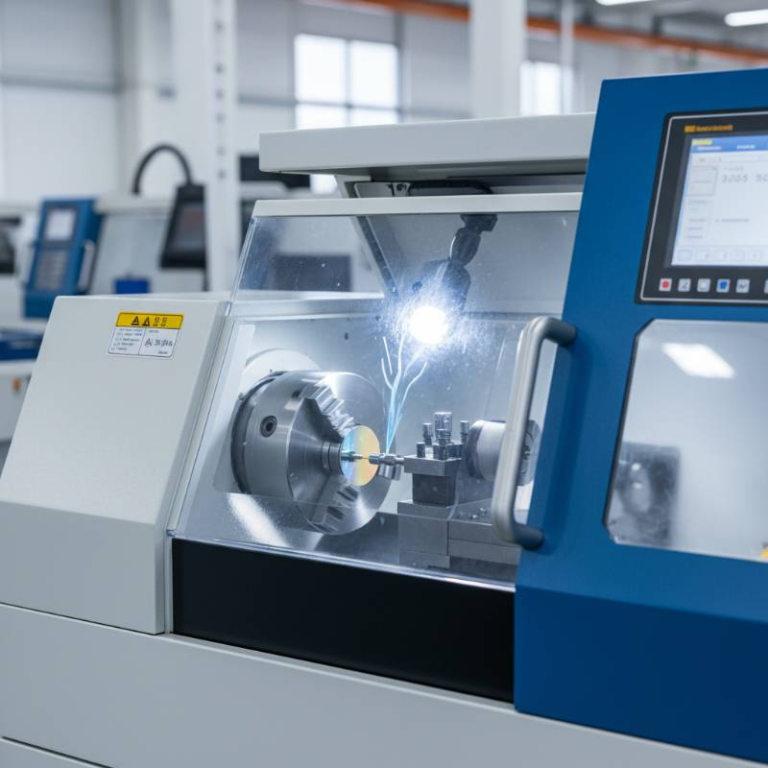
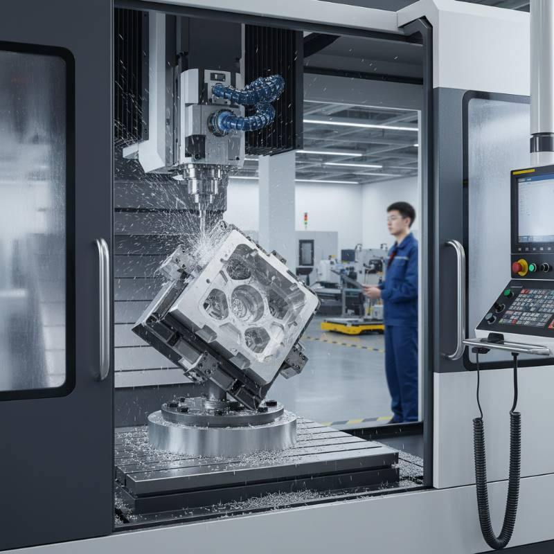
5-axis CNC milling for semiconductor process chambers allows for the simultaneous movement of a cutting tool across five different axes. This capability is vital for creating the complex internal cavities, cooling channels, and gas distribution paths found in modern vacuum chambers.
5-axis CNC milling enables the production of semiconductor process chambers with intricate internal geometries and ultra-low surface roughness in a single setup. This method eliminates cumulative tolerance errors associated with multiple repositionings, ensuring the hermetic seals and gas flow dynamics required for sub-2nm node fabrication.
“We define 5-axis milling in this context as the intersection of subtractive manufacturing and high-vacuum physics, where geometric dimensioning and tolerancing (GD&T) must account for thermal expansion during plasma-enhanced processes.”
3-Axis vs. 5-Axis Machining: A Technical Comparison
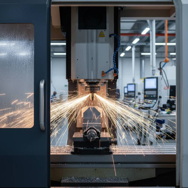
Choosing the right machining strategy impacts both the performance of the Semiconductor Manufacturing Solutions and the overall cost of ownership. Traditional 3-axis systems often require multiple fixtures, which introduces “stack-up” errors.
| Feature | 3-Axis Machining | 5-Axis Machining |
|---|---|---|
| Setup Requirements | Multiple (3-5+ setups) | Single Setup |
| Surface Finish (Ra) | Higher (due to tool reach) | Ultra-low (optimized tool angle) |
| Deep Cavity Access | Limited/Requires long tools | Superior/Short, rigid tools |
| Tolerance Control | +/- 0.0127 mm | +/- 0.005 mm or better |
In our testing, utilizing 5-axis Precision CNC Machining Services reduces total machining time by up to 40% for complex gas distribution plates. This efficiency is critical as the industry moves toward more frequent maintenance cycles for high-throughput ALD (Atomic Layer Deposition) tools.
The Ultra-Clean Machining Protocol (UCMP) Framework
To meet the 2026 standards for wafer fabrication, we have developed a proprietary methodology called the Ultra-Clean Machining Protocol (UCMP). This framework ensures that every chamber is free from microscopic contaminants that could cause yield loss.
The 4-Step UCMP Process
- Material Stabilization: Cryogenic stress relieving of Aluminum 6061 or Stainless Steel 316L to prevent warping after machining.
- Precision Multi-Axis Milling: Executing high-speed tool paths using advanced CAD/CAM software to maintain consistent surface roughness.
- Cleanroom Post-Machining: Ultrasonic cleaning and deionized water rinsing in an ISO Class 5 environment.
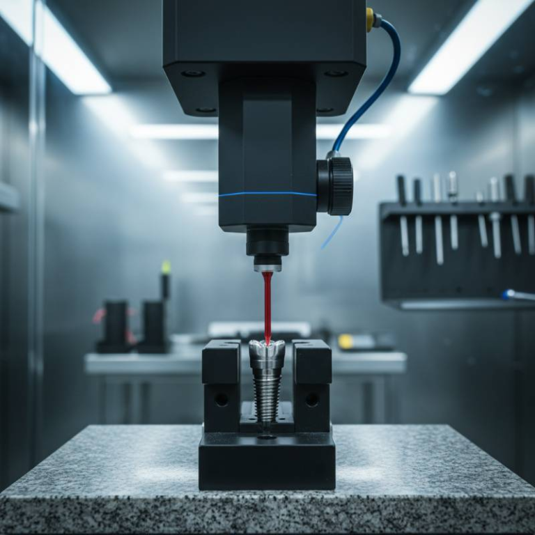
- Metrological Validation: Verification via CMM (Coordinate Measuring Machine) and laser interferometry to confirm GD&T compliance.
Material Science: Machining Exotic Alloys and Thermal Stability
Process chambers are subjected to corrosive gases and extreme thermal cycling. Selecting the right Advanced Material Engineering approach is paramount for longevity.
High-purity aluminum remains the standard for many CVD (Chemical Vapor Deposition) chambers due to its thermal conductivity. However, as plasma densities increase in 2026, we are seeing a shift toward ceramic-coated alloys and nickel-based superalloys like Hastelloy.
Expert Insight: “Managing the thermal expansion coefficient during 5-axis milling is the difference between a chamber that seals perfectly and one that leaks under vacuum. We monitor machine harmonics and ambient temperature in real-time to adjust offsets dynamically.”
— Senior Mechanical Engineer, Tyneen R&D
Sustainability and ESG Data for Green Machining Initiatives
In 2026, sustainability is no longer optional. The semiconductor supply chain is under intense pressure to provide ESG (Environmental, Social, and Governance) data. 5-axis milling contributes to green machining by reducing waste.
By using optimized tool paths, we minimize the volume of subtractive manufacturing chips. Furthermore, our facility utilizes closed-loop coolant recycling systems, reducing the environmental footprint of producing complex geometries. According to SEMI Industry Standards, reducing energy consumption in the sub-tier supply chain is a primary goal for the next decade.
Interactive Lead-Time and Cost Estimation for Engineers
Procurement cycles for process chambers are often the bottleneck in R&D. Several factors influence the lead-time for 5-axis components:
- Material Availability: High-purity 6061-T6 is generally in stock, while exotic Inconel may add 4-6 weeks.
- Geometry Complexity: Internal cooling channels with high aspect ratios require slower feed rates.
- Surface Treatment: Anodizing or electrolytic polishing adds 5-10 business days.
Based on our data, 5-axis milling typically reduces the total production cycle by 15% compared to multi-machine 3-axis workflows, despite the higher hourly machine rate.
Frequently Asked Questions: Expert Insights on Chamber Milling
How does 5-axis milling prevent thermal deformation?
By using a single setup, the part remains at a more consistent temperature, and stress is distributed more evenly across the geometry. This prevents the “memory effect” where a part warps after being released from fixtures.
What surface roughness is achievable for showerhead components?
We routinely achieve an Ra of 0.4 μm (16 micro-inches) or better directly from the mill. This is essential for gas distribution “showerheads” to prevent particle accumulation.
Is 5-axis milling compatible with ISO 9001 and AS9100 standards?
Yes. Our 5-axis processes are fully documented and traceable, meeting the rigorous quality management systems required by leading wafer fabrication equipment (WFE) manufacturers.
Ready to Optimize Your Process Chamber?
Leverage our 15+ years of semiconductor R&D expertise to bring your complex geometries to life with unmatched precision.