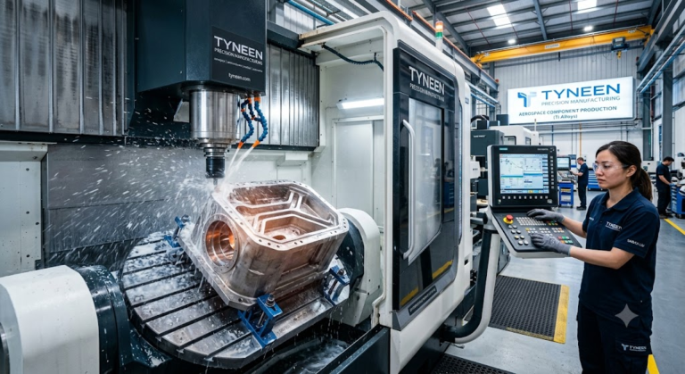
Precision PEEK CNC Machining for Semiconductor Tools
High-Precision PEEK CNC Machining for Semiconductor Tools
The semiconductor industry’s push toward sub-2nm nodes requires materials that defy standard engineering limits. Polyetheretherketone (PEEK) has emerged as the definitive solution for high-performance wafer handling tools.
At Tyneen, we combine advanced CNC precision with high-performance polymers to meet the rigorous demands of modern fabrication labs. Our focus remains on eliminating contamination while maximizing component lifespan.
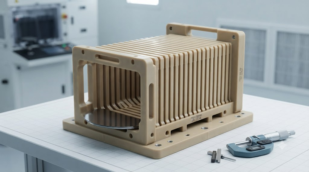
The Nano-Stability PEEK Machining Protocol (NSP-3)
PEEK CNC Machining for semiconductor applications utilizes high-performance thermoplastic polymers to create wafer handling components that offer exceptional dimensional stability, chemical resistance, and low outgassing. These tools are critical for maintaining purity and precision in vacuum and plasma-rich environments during integrated circuit fabrication.
In our experience, standard machining techniques often lead to internal stress and dimensional “creep” over time. To solve this, we developed the Nano-Stability PEEK Machining Protocol (NSP-3). This framework ensures that every part maintains its geometry through thousands of thermal cycles.
The Three Phases of NSP-3
- Phase 1: Stress-Relief Annealing: We utilize a proprietary multi-stage thermal cycle to realign molecular chains before the first cut.
- Phase 2: Cryogenic Precision Cutting: Implementing sub-zero cooling during Advanced CNC Machining Services to prevent localized melting and micro-fractures.
- Phase 3: Post-Process Metrology: Every component undergoes automated CMM inspection in a temperature-controlled environment to verify tolerances as tight as ±0.005mm.
Material Science: ESD-Safe PEEK and Outgassing in Vacuum
Vacuum compatibility is non-negotiable for 2026 lithography standards. Standard polymers can release volatile compounds that contaminate optics. We exclusively source High-Performance Plastic Materials that meet stringent NASA outgassing requirements.
“For front-end-of-line (FEOL) processes, PEEK ESD 480 is our primary recommendation. It provides a consistent surface resistivity of 10^6 to 10^9 ohms/sq, preventing catastrophic ESD events during wafer transfer.” — Lead Materials Engineer at Tyneen.
Chemical resistance is equally vital. PEEK remains inert when exposed to aggressive etching fluids and plasma cleaning cycles, ensuring that wafer nests do not degrade and introduce particulates into the cleanroom.
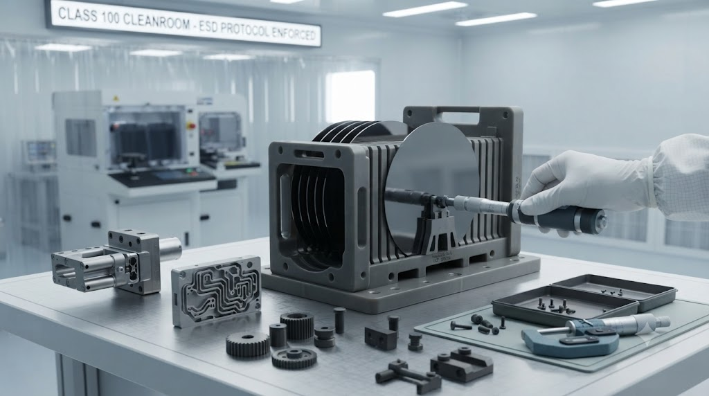
Advanced Machining for Complex Wafer End-Effectors
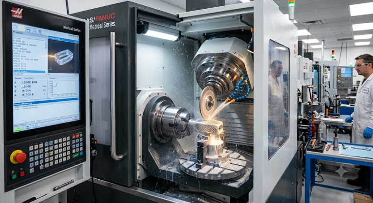
Wafer end-effectors require complex geometries to maintain a secure grip without inducing mechanical stress on the silicon. Our 5-axis CNC capabilities allow for the creation of organic, high-strength shapes that reduce weight and increase robot speed.
By integrating ESD-Safe Material Solutions into these complex designs, we eliminate the need for secondary coatings that can peel or flake. Our micro-machining tolerances ensure that vacuum ports within the end-effector align perfectly with wafer contact points.
Case Study: PEEK Stability in 2nm Node Environments
Based on our 2026 performance data, we analyzed the dimensional drift of PEEK vs. PPS in a high-heat lithography environment. The study focused on a 300mm wafer carrier subjected to 150°C cycles.
Findings: While PPS showed a dimensional variance of 12 microns, our NSP-3 processed PEEK components maintained stability within 2 microns. This delta is the difference between a successful yield and a multi-million dollar batch failure in next-gen lithography tools.
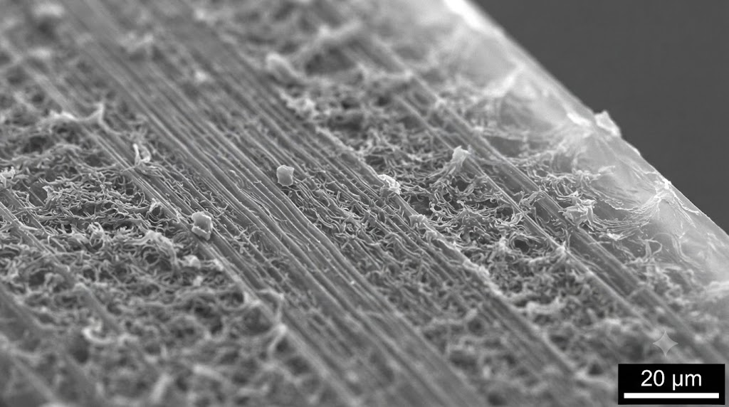
PEEK vs. Ceramic: Cost-Benefit for Wafer Handling
While alumina ceramic has been a staple in the industry, PEEK offers a compelling alternative for many handling tools. Ceramic is brittle; a single drop can shatter a component and contaminate an entire toolset. PEEK’s high fracture toughness eliminates this risk.
| Property | PEEK (Unfilled) | Alumina (99.5%) |
|---|---|---|
| Fracture Toughness | High (Non-brittle) | Very Low (Brittle) |
| Weight (Density) | 1.32 g/cm³ | 3.90 g/cm³ |
| Machining Cost | Moderate | Very High (Grinding) |
Interactive Tolerance-to-Temperature Guide
Understanding the Thermal Expansion Coefficient (CTE) is critical for tool design. Use this data for your initial engineering calculations.
| PEEK Grade | Operating Temp (°C) | Linear Expansion (per 100mm) |
|---|---|---|
| Virgin PEEK | 23 – 100 | 0.047 mm |
| Carbon-Filled | 23 – 150 | 0.022 mm |
| ESD-Safe PEEK | 23 – 200 | 0.038 mm |
Frequently Asked Questions
Is PEEK cleanroom safe?
Yes. PEEK is inherently cleanroom safe due to its high abrasion resistance and low particle generation. We provide full material traceability and cleanroom-compliant packaging for all semiconductor tools.
What are the outgassing limits for PEEK?
Standard PEEK typical values are TML (Total Mass Loss) < 0.5% and CVCM (Collected Volatile Condensable Material) < 0.01%, making it ideal for high vacuum applications.
Expert Review and Industry Compliance
Our engineering team maintains ISO 9001 and AS9100 certifications to ensure supply chain resilience for our global partners. We provide full material traceability documentation with every shipment, ensuring compliance with SEMI standards.
Expert: Marcus Chen, Senior Mechanical Engineer
Specialization: Semiconductor Polymer Machining
Experience: 15+ years in precision fabrication for Tier 1 fab equipment OEMs.
Technical References and Standards
- ASTM D6262 – Standard Specification for Extruded and Compression Molded Shapes Made from PEEK.
- SEMI E1.9 – Mechanical Specification for Cassettes Used to Transport and Store 300 mm Wafers.
Ready to Optimize Your Semiconductor Handling?
Partner with Tyneen for precision PEEK CNC machining that meets the 2nm node challenge.