Precision Grinding for Semiconductor Wafer Chucks
Precision Grinding for Semiconductor Wafer Chucks: Engineering Overview
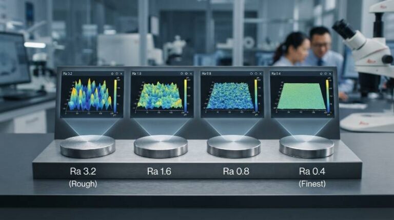
Precision grinding for semiconductor wafer chucks is the ultra-precision machining process used to achieve sub-micron global flatness, precise surface roughness (Ra < 0.05 µm), and defect-free geometries on technical ceramic and metal matrix workpieces. This machining accuracy ensures uniform thermal dissipation, reliable electrostatic clamping, and depth-of-focus control during front-end wafer fabrication processes.
In modern photolithography, plasma etch, and chemical mechanical planarization (CMP), the semiconductor wafer chuck serves as the primary mechanical and thermal reference plane for 200mm and 300mm silicon wafers. Even nanoscale deviations in chuck planarity propagate through the wafer stack, causing localized focal plane distortion, overlay errors, and uneven plasma distribution.
At advanced technology nodes below 5nm, wafer holding chuck flatness directly dictates lithographic yield. Electrostatic chucks (ESCs) and vacuum chucks must maintain total coplanarity under harsh vacuum and plasma conditions while resisting process-induced thermal degradation. Tyneen integrates high-precision grinding technologies with specialized tooling to deliver advanced industry tooling solutions that meet the stringent standards of the global semiconductor supply chain.
Critical Engineering Metrics: Surface Roughness, Flatness, and TIR
Semiconductor wafer chuck manufacturing demands geometric tolerances that push the limits of conventional mechanical engineering. Controlling chuck topography prevents mechanical stress concentrations that trigger wafer backside scratching, particle generation, or wafer breakage during high-speed vacuum clamping.
Geometric tolerances must be maintained across broad environmental operating envelopes, from cryogenic cooling stages to high-temperature chemical vapor deposition (CVD) environments exceeding 400°C.
According to Semiconductor Equipment and Materials International (SEMI) standards, the allowable non-planarity for lithography-grade wafer clamping fixtures must not exceed 0.5 µm Total Indicator Reading (TIR) across a standard 300mm chuck diameter.
| Metric Parameter | 200mm Wafer Chuck | 300mm Advanced ESC | Functional Impact on Wafer Fab |
|---|---|---|---|
| Total Thickness Variation (TTV) | < 1.0 µm | < 0.3 – 0.5 µm | Eliminates focus blur and focal plane tilt in EUV/DUV steppers. |
| Total Indicator Reading (TIR / Flatness) | < 1.2 µm | < 0.5 µm | Prevents wafer bowing and uniform helium backside pressure leakage. |
| Surface Roughness (Ra) | < 0.1 µm | < 0.02 – 0.05 µm | Minimizes backside micro-scratching and particle contamination. |
| Mean Peak-to-Valley Height (Rz) | < 0.5 µm | < 0.2 µm | Ensures absolute contact integrity for high-voltage electrostatic clamping. |
| Embossed Mesa / Pin Coplanarity | ± 0.5 µm | ± 0.2 µm | Guarantees uniform clamping force and symmetrical thermal conductivity. |
Advanced Ceramic Materials for Wafer Chucks: Machining Characteristics
Semiconductor wafer chucks rely on high-purity technical ceramics and engineered refractory compounds to survive corrosive halogen plasma gases, high-voltage dielectric stresses, and extreme thermal cycling. Each ceramic material presents distinct mechanical grinding challenges due to high fracture toughness combined with extreme hardness.
High-Purity Alumina (99.5%+ Al2O3)
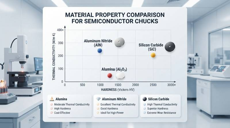
Alumina remains a widely deployed dielectric material for standard vacuum and electrostatic chuck bodies. It offers high dielectric strength (> 15 kV/mm) and excellent chemical resistance, but its high hardness (HV 1500–1800) demands diamond grinding wheels with precise bond friability to prevent surface thermal shocking.
Aluminum Nitride (AlN)
AlN is preferred in high-temperature wafer processing chambers due to its high thermal conductivity (170–220 W/m·K) paired with a coefficient of thermal expansion (CTE) closely matched to silicon (4.5 × 10⁻⁶/K). Grinding AlN requires tight coolant chemistry control, as the material can undergo grain pull-out if wheel dressing is uneven.
Silicon Carbide (CVD-SiC and Sintered SiC)
Chemical Vapor Deposition Silicon Carbide (CVD-SiC) and sintered SiC provide the highest stiffness-to-weight ratio (E > 400 GPa) and extreme plasma erosion resistance. SiC is notoriously abrasive and brittle, requiring high-rigidity CNC grinding platforms and specialized diamond tooling to avoid micro-chipping along gas channels and edge perimeters.
Kinematic Diamond Grinding Mechanics: Eliminating Brittle Micro-Cracks
Traditional grinding of technical ceramics often operates in the brittle fracture regime, where material removal occurs via median and lateral crack propagation. For semiconductor wafer chucks, subsurface cracks as small as 2 µm can cause catastrophic vacuum seal failure or localized dielectric breakdown during wafer processing.
To eliminate subsurface damage, precision grinding must operate within the ductile-regime grinding mode. In our manufacturing experience, by restricting the critical uncut chip thickness ($d_c$) below the ceramic’s critical transition threshold (typically $d_c < 100\text{ nm}$ for SiC and AlN), the material undergoes plastic shear deformation rather than brittle fracture.
Engineering Insight: Ductile-regime machining of CVD-SiC requires high-rigidity spindles with dynamic runout below 0.1 µm, high peripheral wheel speeds ($v_s \ge 35\text{ m/s}$), and precision vitrified diamond wheels with grit sizes ranging from #1500 to #3000 mesh.
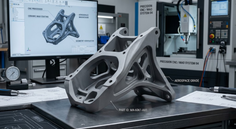
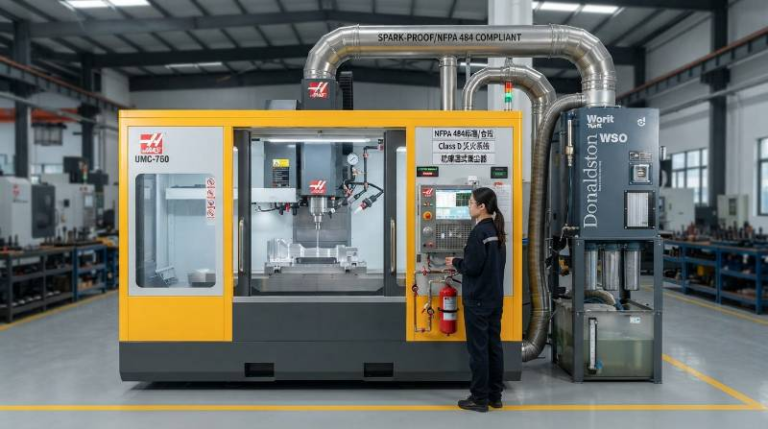
Diamond wheel truing and dressing protocols are equally vital. In-situ rotary diamond dressers ensure wheel roundness within 0.2 µm, while continuous high-pressure coolant flushing (minimum 1.5 MPa) prevents wheel loading and minimizes thermal gradients during continuous surface passes. Tyneen pairs these kinematics with advanced multi-axis platforms, delivering world-class precision CNC machining services tailored for semiconductor-grade ceramics.
The Tyneen Ultra-Flat Chuck Protocol (UFG-Protocol™)
To achieve sub-micron coplanarity while eliminating subsurface micro-cracks across entire chuck surfaces, Tyneen utilizes a proprietary manufacturing framework: The Tyneen Ultra-Flat Chuck Protocol (UFG-Protocol™). This 5-stage framework ensures deterministic quality from initial ceramic blank preparation through cleanroom certification.
- Finite Element Analysis (FEA) & Thermal Stress Relief:
Every chuck blank undergoes thermal profiling and FEA modeling to simulate mechanical clamping stress and thermal gradients. Sub-critical stress-relief annealing stabilizes the ceramic crystal matrix before rough cutting. - Multi-Axis CNC Rough Contouring:
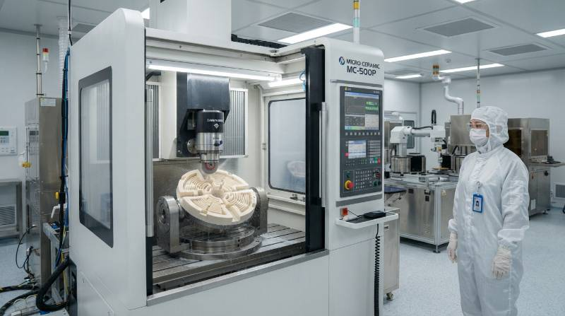
High-rigidity multi-axis CNC machines mill the overall outer geometry, base mounting interfaces, and coarse lift-pin clearance holes using coarse diamond-impregnated rotary cutters under flooded synthetic cooling. - Ductile-Regime Diamond Micro-Grinding:
The primary clamping face is processed on hydrostatically mounted surface grinders using vitrified-bond diamond wheels (grit #1200 to #3000). Feed steps are limited to sub-micron increments to maintain plastic deformation cutting kinematics. - Dynamic Double-Sided Lapping & CMP Polishing:
High-precision double-sided planetary lapping with customized polycrystalline diamond slurry balances surface stress on both faces. A final Chemical Mechanical Polishing (CMP) step reduces surface roughness to $Ra < 0.02\text{ µm}$. - Metrology Certification:
Every finished chuck undergoes 100% full-surface 3D laser interferometry and tactile CMM measurement inside an ISO Class 5 cleanroom environment.
Vacuum Grooves, Gas Channels, and Micro-Pinhole Feature Machining
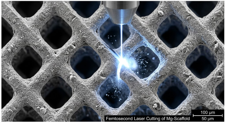
Electrostatic chucks require complex backside gas distribution patterns—including spiral micro-channels for helium cooling and arrays of embossed support pins (mesas). These geometries must be machined into hard ceramic substrates without edge chipping or micro-burrs.
Tyneen employs ultra-high-speed (up to 60,000 RPM) air-bearing micro-grinding spindles paired with micron-diameter diamond electroplated tools. Ultrasonic-assisted CNC grinding is deployed for high-aspect-ratio wafer lift-pin holes, reducing tool engagement force by up to 60% and guaranteeing crack-free hole rims.
Advanced Metrology: Optical Interferometry and High-Precision CMM
Validating sub-micron chuck planarity requires non-contact, high-resolution metrology that eliminates measurement artifacts caused by probe contact force or environmental thermal fluctuations. Testing must conform to rigorous dimensional validation standards, such as those established by ISO/TC 213 Geometrical Product Specifications.
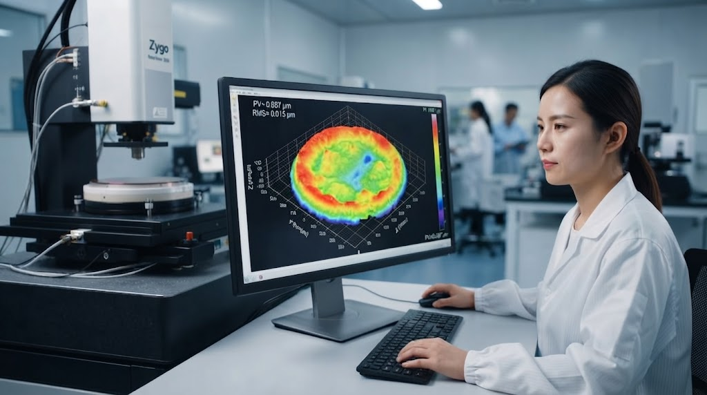
Our quality assurance workflow deploys three complementary metrology technologies to ensure full-surface compliance:
- Large-Aperture Laser Interferometry: Full-aperture Fizeau interferometers map the entire 300mm clamping surface in seconds, providing 3D wavefront phase maps with height resolution down to 0.1 nm.
- White Light Optical Profilometry: Non-contact scanning interferometry measures micro-groove wall profiles, helium sealing dam flatness, and pin array height consistency at nanometer-level vertical resolution.
- Multi-Point High-Precision CMM: Bridge-type coordinate measuring machines equipped with low-force scanning probes verify datum coplanarity, vacuum port alignment, and structural bolt-hole locations across the chuck base.
Refurbishment, Re-Lapping, and Re-Grinding Lifecycle Programs
High-density plasma etching with aggressive fluorocarbon and chlorine chemistries causes gradual physical erosion and dielectric coating degradation on electrostatic chuck surfaces. Replacing an entire ceramic ESC assembly represents significant capital expenditure and extensive fab downtime.
Tyneen offers structured wafer chuck refurbishment programs that restore damaged or worn chucks back to OEM tolerances, extending total operational lifecycle by up to 300%.
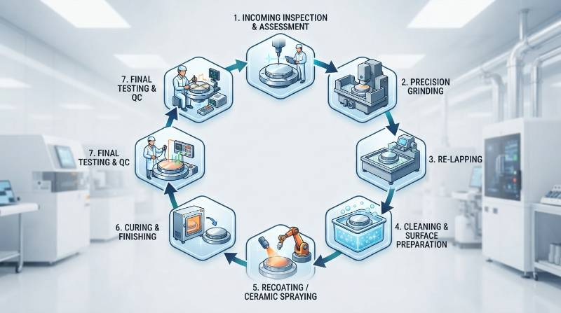
The refurbishment procedure involves five controlled steps:
- Incoming Metrology & Defect Mapping: High-resolution optical profiling identifies plasma erosion depth, seal ring degradation, and localized micro-arcing damage.
- Controlled Surface Skim-Grinding: Ultra-precision CNC grinding strips the damaged ceramic or dielectric layer (typically removing 15–30 µm of base material) while re-establishing datum parallelism.
- Dielectric Recoating: Thermal spray or aerosol deposition applies high-purity Al2O3, Y2O3 (Yttria), or AlN dielectric coatings tailored for plasma resistance.
- Final Re-Grinding & Micro-Lapping: The newly applied coating is ground and lapped down to final thickness, restoring strict flatness (< 0.5 µm) and pin height uniformity.
- Dielectric Breakdown & Vacuum Leak Testing: Chucks undergo high-voltage insulation breakdown testing (up to 5 kV DC) and helium mass spectrometer leak detection.
Cleanroom Processing, Contamination Control, and Fab Packaging
A single metallic ion or 0.1 µm particulate residue remaining on a precision-ground wafer chuck can contaminate an entire semiconductor production batch. Therefore, post-grinding cleaning and packaging must meet stringent fab standards.
Following final metrology, wafer chucks are transferred directly into an ISO Class 5 (Class 100) cleanroom environment. The chucks undergo multi-stage ultrasonic cleaning cycles using 18.2 MΩ·cm Ultra-Pure Water (UPW) and specialized non-ionic surfactants to remove all residual slurry, abrasive diamond grains, and organic films.
Post-cleaning validation includes Liquid Particle Counting (LPC) and Ion Chromatography to verify ionic cleanliness down to parts-per-billion (ppb) thresholds. Every component is then vacuum-sealed within double-layer static-dissipative polyethylene bags with cleanroom-certified nitrogen purging and packaged inside shock-isolated crates for global shipment.
Custom Wafer Chuck Manufacturing & DFM Solutions by Tyneen
Whether you require rapid turnaround prototypes for next-generation wafer handling tools or high-mix, low-volume production of CVD-SiC and AlN electrostatic chucks, Tyneen delivers comprehensive ultra-precision manufacturing solutions. Our integrated production facilities bridge the gap between engineering concept and fab-ready semiconductor hardware.
Our engineering team provides upfront Design for Manufacturability (DFM) reviews to optimize cooling channel geometries, reduce ceramic stress risers, and cut machining cycle times. Leveraging our rapid prototyping capabilities, we assist semiconductor equipment OEMs and advanced fabs in iterating and scaling complex chuck designs with minimal lead times.
Frequently Asked Questions (FAQs)
What surface flatness is required for a 300mm semiconductor wafer chuck?
A 300mm lithography-grade wafer chuck generally requires a Total Indicator Reading (TIR) flatness of less than 0.5 µm and a Total Thickness Variation (TTV) under 0.3 µm. Plasma etch and inspection chucks can operate with flatness tolerances between 0.5 µm and 1.2 µm depending on the specific process node.
Why is CVD Silicon Carbide (SiC) preferred over Alumina for high-power etching chucks?
CVD-SiC offers significantly higher thermal conductivity (up to 270 W/m·K vs. ~30 W/m·K for Alumina), exceptional mechanical stiffness, and superior resistance to corrosive halogen plasma erosion. This enables superior wafer backside temperature uniformity during high-power RF plasma processing.
Can worn electrostatic chucks (ESCs) be re-ground without losing structural integrity?
Yes. By utilizing controlled skim-grinding and re-lapping, technicians remove only 15 to 30 µm of the eroded ceramic surface layer. The chuck is then recoated with high-purity dielectric material and precision ground back to OEM geometric tolerances, saving up to 60% compared to new component costs.
How does Tyneen prevent subsurface micro-cracks during ceramic grinding?
Tyneen applies the proprietary UFG-Protocol™, maintaining ductile-regime grinding kinematics with sub-micron feeds, ultra-fine vitrified diamond wheels (#1500–#3000 mesh), stabilized hydrostatic spindle platforms, and high-pressure flood coolant delivery to ensure plastic shear deformation without crack propagation.
Ready to Optimize Your Semiconductor Tooling Tolerances?
Partner with Tyneen for ultra-precision grinding, technical ceramic machining, and custom wafer chuck manufacturing engineered to sub-micron standards.