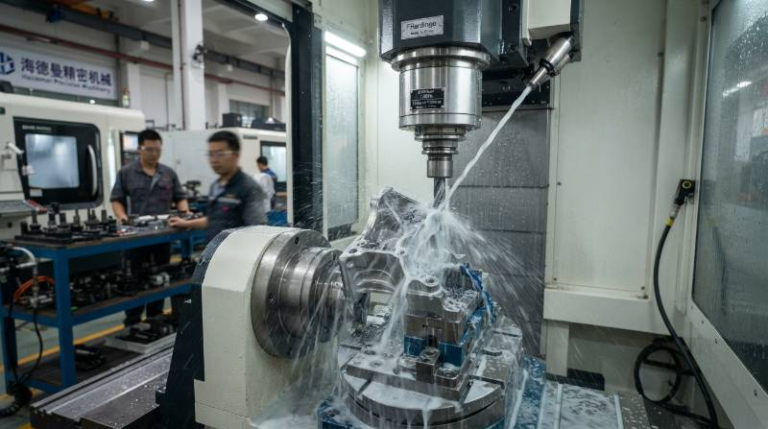
Sheet Metal Fabrication for Semiconductor Equipment Enclosures
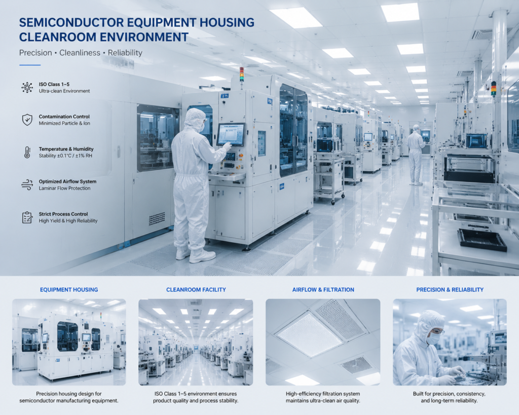
What is Semiconductor-Grade Enclosure Fabrication?
Semiconductor-grade enclosure fabrication is a specialized manufacturing process that produces high-purity, high-tolerance equipment housings. These units utilize 304/316L stainless steel and advanced Precision Engineering Services to ensure zero-particle shedding and structural stability under high-vacuum conditions.
In our experience, the difference between success and failure in the fab lies in the details. We define semiconductor-grade by three pillars: ultra-low outgassing, sub-millimeter geometric tolerances, and ESD-safe surface finishes.
“At the 2nm node, a single molecular layer of outgassed vapor can ruin an entire wafer batch. Fabrication isn’t just about bending metal; it’s about molecular-level hygiene.” — Senior Materials Scientist.
The UHP-Shield™ Framework: Our Proprietary Fabrication Protocol
To meet the rigorous demands of 2026 fab environments, we developed the UHP-Shield™ Protocol. This methodology ensures that every enclosure exceeds baseline industry expectations.
- AI-Driven DFM: We use predictive algorithms to identify potential stress points or “dirt traps” in the design phase.
- Orbital TIG Welding: Automated welding ensures consistent, deep penetration with zero porosity, preventing gas pockets.
- Chemical Passivation: A multi-stage process that removes free iron from the surface, maximizing corrosion resistance.
- Cleanroom Packaging: Final assembly and double-bagging occur within an ISO Class 10 environment to prevent transit contamination.
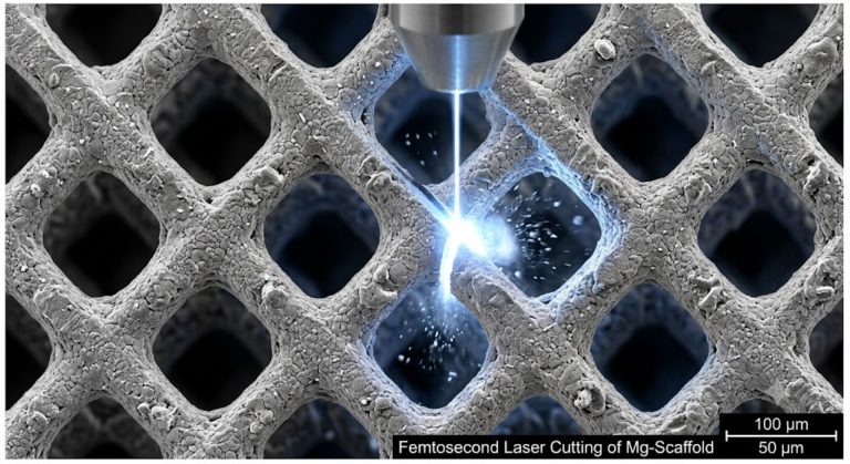
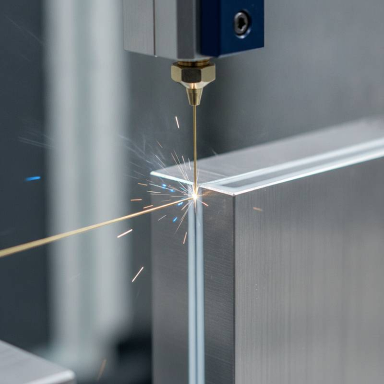
This protocol is the result of our deep vertical integration. By controlling the process from CNC laser cutting to final inspection, we maintain total traceability.
Material Science for 2nm Nodes: Preventing Outgassing
Outgassing is the silent killer of semiconductor yield. When materials are placed under vacuum, they release trapped gases that condense on the wafer surface.
We prioritize 316L stainless steel for its superior resistance to corrosive process gases. Furthermore, powder coating outgassing is a major concern; we utilize specialized low-outgassing coatings or electropolished finishes to mitigate this risk.
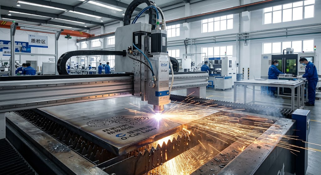
Our data shows that 316L Stainless Steel with an electropolished finish (Ra < 0.2µm) significantly reduces particle adhesion. This is critical for Wafer Fabrication Equipment operating in high-vacuum or high-temperature zones.
Engineering for Cleanroom Compliance: ISO 14644 and SEMI Standards
Compliance is non-negotiable. Enclosures must align with Cleanroom Material Standards to ensure they do not introduce contaminants into the fab.
| Finish Type | ISO Class Support | ESD Safety | Outgassing Level |
|---|---|---|---|
| Electropolished 316L | Class 1 – 10 | Excellent | Ultra-Low |
| ESD Powder Coating | Class 100 – 1000 | Certified | Low |
| Anodized Aluminum | Class 10 – 100 | Good | Moderate |
Adherence to SEMI S2 (Safety Guidelines) and SEMI S8 (Ergonomics) is verified through rigorous testing. These standards, published by SEMI, are the benchmark for equipment safety in the microelectronics industry.
Advanced Thermal Management and EMI/RFI Shielding
As AI-chip production ramps up, power densities within enclosures are skyrocketing. We integrate Advanced Thermal Management solutions directly into the sheet metal chassis.
This includes liquid-cooling channels embedded within modular frame assemblies and optimized airflow patterns designed through CFD simulation. Furthermore, EMI/RFI shielding is critical to prevent electronic interference from disrupting the sensitive lithography process.
We use specialized conductive gaskets and honeycomb vents to ensure the enclosure acts as a perfect Faraday cage, maintaining signal integrity for the internal sensors.
Modular vs. Monolithic: Scaling Your Wafer Fab Equipment
In 2026, the industry is moving away from monolithic, “all-in-one” enclosures. Instead, modular designs have become the gold standard for rapid fab scaling.
Modular enclosures allow for:
- Parallel Assembly: Different modules can be fabricated and tested simultaneously.
- Ease of Maintenance: Individual sections can be swapped without dismantling the entire tool.
- Rapid Scaling: New process chambers can be added to existing frames with minimal downtime.
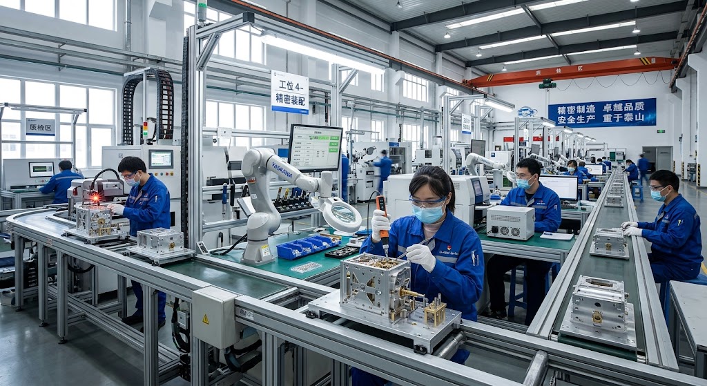
Achieving sub-millimeter tolerances across these modular interfaces requires AS9100-certified quality systems. Our frames use precision-machined mating surfaces to ensure perfect alignment upon assembly.
Geopolitical De-risking: Near-Shoring Your Supply Chain
The semiconductor landscape is shifting toward regional resilience. Geopolitical de-risking has led many OEMs to move away from long-distance supply chains in favor of near-shoring.
By partnering with a vertically integrated fabricator, companies can reduce lead times and ensure material certification transparency. We provide full documentation for every heat of steel used, ensuring compliance with global trade regulations and sustainability mandates.
Frequently Asked Questions
What are the typical lead times for custom semiconductor enclosures?
Lead times vary based on complexity. Standard modular frames typically ship in 4-6 weeks, while complex, UHP-validated enclosures requiring custom prototyping may take 10-12 weeks.
Why is AS9100 certification important for semiconductor fabrication?
AS9100 ensures a level of quality management and traceability that exceeds standard ISO 9001 requirements, which is essential for the zero-defect culture of the semiconductor industry.
What tolerance standards do you follow?
We primarily work to ISO 2768 fine/medium standards. For critical mating surfaces, we achieve sub-millimeter precision through CNC machining post-welding.
About the Author: Expert in Semiconductor Mechanical Design
This technical guide was reviewed by our Lead Mechanical Engineer (Semiconductor Division). With over 15 years of experience in Wafer Fabrication Equipment design, they have overseen the deployment of enclosure systems for three major global foundries. Their expertise ensures that every project adheres to the highest levels of structural and chemical integrity.
References and Technical Standards
- ISO 14644: Cleanrooms and associated controlled environments.
- SEMI S2-0715: Environmental, Health, and Safety Guideline for Semiconductor Manufacturing Equipment.
- SEMI S8: Safety Guideline for Ergonomics Engineering of Semiconductor Manufacturing Equipment.
- Material Science White Paper: “Outgassing Characteristics of Stainless Steel in High Vacuum.”