Precision Grinding for Semiconductor Wafer Chucks | Tyneen
Understanding Precision Grinding in Semiconductor Wafer Chuck Manufacturing
Precision grinding for semiconductor wafer chucks is an ultra-precision abrasive machining process designed to achieve sub-micron surface flatness (TIR < 0.5 µm) and nanometer-scale surface roughness across technical ceramic, metal-matrix, and hybrid dielectric clamping plates. This process establishes the essential mechanical datum required to prevent wafer slippage, focal plane distortion in extreme ultraviolet (EUV) lithography, and localized thermal gradients during chemical mechanical planarization (CMP) and plasma etching.
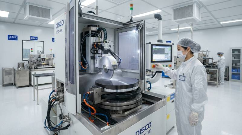
In modern wafer fabrication, semiconductor wafer chucks serve as the physical interface holding delicate silicon, gallium nitride (GaN), and silicon carbide (SiC) wafers during critical processing steps. Chuck architectures range from classic mechanical pin arrays and vacuum chucks to complex Coulombic and Johnsen-Rahbek electrostatic chucks (ESCs).
Any dimensional variance or microscopic topography error on the chuck surface directly maps onto the processed wafer. A localized 1 µm chuck high-spot causes depth-of-focus (DOF) yield failure in advanced lithography nodes below 3 nm. Modern fabs rely heavily on specialized advanced machining services to meet these stringent structural demands.
Semiconductor Metrology Definition: Wafer Chuck Total Indicated Runout (TIR) represents the absolute peak-to-valley variance across the entire functional chuck surface. Per SEMI M1 and SEMI E10 standards, high-density chuck platforms must maintain a global TIR under 0.5 µm and localized slope variation below 0.1 µm per 20 mm.
Material Dynamics: Sintered SiC vs. AlN vs. Porous Dielectrics
Semiconductor wafer chuck substrates must balance extreme hardness, high thermal conductivity, and coefficient of thermal expansion (CTE) matching with processed silicon. Grinding these materials requires crossing the ductile-to-brittle transition regime to avoid subsurface fracture.
Sintered Silicon Carbide (SiC) delivers extreme flexural modulus (400–450 GPa) and thermal conductivity (up to 270 W/m·K), making it ideal for high-power plasma etching chucks. However, its hardness (Knoop ~2500 kg/mm²) rapidly glazes standard wheels, requiring vitrified diamond wheels with controlled porosity to manage cutting forces. Read more about selecting semiconductor ceramic materials.
Aluminum Nitride (AlN) provides superior dielectric properties and a CTE (~4.5 × 10⁻⁶/K) closely matched to silicon, widely serving in electrostatic chuck bases. AlN is mechanically softer than SiC but highly susceptible to grain pull-out and edge micro-chipping during rotary grinding passes.

| Property / Parameter | Sintered Silicon Carbide (SiC) | Aluminum Nitride (AlN) | Porous Alumina Matrix (Al₂O₃) |
|---|---|---|---|
| Thermal Conductivity | 150 – 270 W/m·K | 170 – 220 W/m·K | 25 – 35 W/m·K |
| Vickers Hardness (HV) | 22 – 28 GPa | 10 – 12 GPa | 14 – 18 GPa |
| Critical Ductile Depth (dc) | ~15 – 35 nm | ~40 – 80 nm | Grain Boundary Dependent |
| Recommended Diamond Bond | Porous Vitrified / Cast Iron Metal | Resin / Hybrid Metal Bond | Resinoid Fine Mesh (#2000+) |
| Target Achievable Ra | < 0.015 µm | < 0.035 µm | < 0.080 µm |
Sub-Micron Geometric Tolerances and Surface Metrology
Semiconductor chuck metrology requires verifying three concurrent parameters: global flatness across the full 300 mm diameter, localized coplanarity across support pins (mesas), and surface roughness according to ASME B46.1 Surface Metrology Standards.
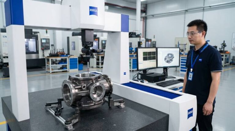
In our manufacturing experience, relying strictly on contact coordinate measuring machines (CMMs) introduces contact deflection errors on micro-pin arrays. We verify chuck geometry through multi-wavelength phase-shifting interferometry and non-contact chromatic confocal sensors housed in temperature-stabilized environments maintained at 20.0 ± 0.1°C.
Engineering Insight: Achieving an Ra < 0.02 µm on sintered SiC without micro-scratches requires precise acoustic emission (AE) monitoring. Real-time AE sensors detect the onset of brittle grain micro-fracture within 5 milliseconds, enabling automatic feed-rate adjustments before micro-cracks propagate into the dielectric layer.
CNC Kinematics: Spindle Pitch, Tilt Compensation, and Micro-Profiling
Grinding large-diameter wafer chucks requires rigid ultra-precision multi-axis CNC surface grinders equipped with aerostatic or hydrostatic bearing spindles. Hydrostatic spindles eliminate micro-vibrations, maintaining dynamic spindle runout below 0.03 µm at 6,000 RPM.
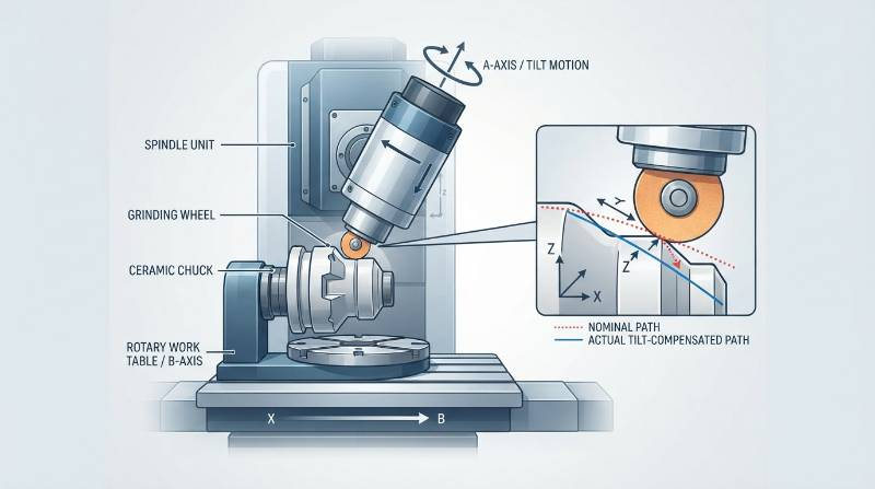
Active spindle tilt compensation corrects for thermal expansion drift along the vertical Z-axis and cross-slide angularity errors. When finishing pin-array chucks (mesa patterns) or concentric vacuum distribution channels, the grinder utilizes 5-axis synchronized micro-interpolation.
Micro-grooves and helium cooling ports require specialized peripheral diamond profiling wheels. Wheel edge radii must remain below 10 µm throughout the cycle to prevent chipping at the vacuum channel boundary edges.
Mitigating Subsurface Damage (SSD) and Thermal Stresses
Subsurface damage (SSD)—consisting of micro-cracks, grain boundary dislodgement, and residual tensile stresses—drastically degrades dielectric breakdown voltage in electrostatic chucks. If SSD depth exceeds 2 µm, the chuck risks dielectric breakdown under high-voltage RF bias conditions.
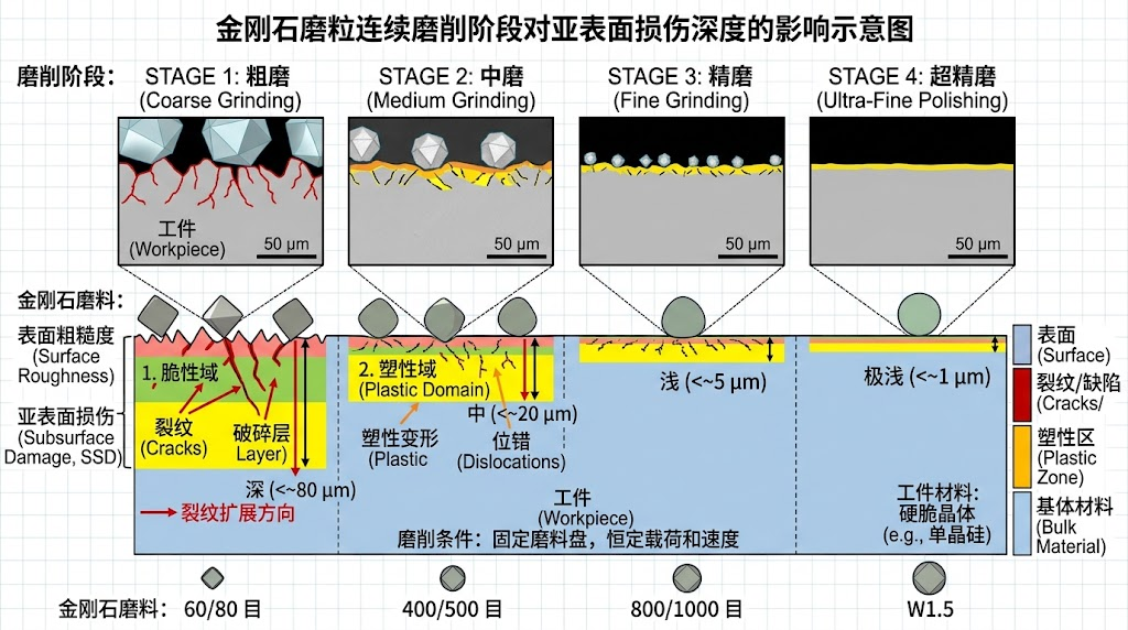
Eliminating SSD requires continuous electrolytic in-process dressing (ELID) or synchronized rotary diamond truing to keep diamond abrasive grains sharp and free of swarf loading. Dull abrasives increase grinding zone temperatures above 400°C, causing localized phase transformation and micro-cracking in AlN substrates.
Thermally managed synthetic coolant, delivered through coherent-jet nozzles at matched wheel surface velocities (30–45 m/s), flushes swarf immediately and keeps thermal variation across the workpiece below 0.2°C.
The Tyneen 4S-MCG Protocol: Turnkey Hybrid Chuck Manufacturing
To ensure high dimensional repeatability and surface integrity, our engineering team executes the Proprietary Tyneen 4-Stage Sub-Micron Chuck Grinding Protocol (4S-MCG). This methodology bridges the gap between rough structural manufacturing and nanoscale finishing.
Stage 1: Multi-Axis Pre-Forming & Internal Manifold Milling
Substrate blocks undergo multi-axis precision CNC milling to form internal helium channels, vacuum manifolds, and mounting datums prior to final sintering or hard-state grinding.
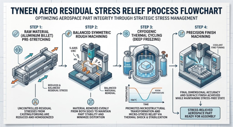
Stage 2: Stress-Relief Annealing & Semi-Finish Rotary Grinding
Workpieces pass through high-vacuum thermal stabilization cycles to neutralize residual stresses. Semi-finish rotary surface grinding uses #600 to #1000 vitrified diamond wheels to establish datum planar alignment within 1.5 µm TIR.
Stage 3: Ductile-Regime Ultra-Precision Rotary Surface Grinding
Utilizing high-stiffness hydrostatic spindles, depth of cut is locked below the critical ductile transition depth ($d_c \le 25\text{ nm}$). This eliminates brittle fracture propagation, yielding Ra < 0.02 µm and TIR < 0.3 µm across 300 mm platforms.
Stage 4: Micro-Pin Profiling, In-Situ Metrology & ISO Class 5 De-Swarf
Micro-pin arrays and gas relief pockets are precision ground with micron-profile diamond points. Parts undergo non-contact white light interferometric scanning followed by multi-frequency ultrasonic de-swarfing in an ISO Class 5 cleanroom.
Cleanroom Post-Processing, Reconditioning, and ESC Refurbishment
Wafer chuck longevity is maintained through structured refurbishing workflows. During fab operation, plasma exposure erodes dielectric coatings and alters surface profile geometries.
Refurbishment involves stripping residual coatings, re-grinding the ceramic face to restore planarity to < 0.5 µm TIR, re-depositing high-purity Yttria ($Y_2O_3$) or Alumina ($Al_2O_3$) dielectric layers via thermal spray or PVD, and conducting a final ductile-mode kiss-grinding pass.
Completed chucks undergo multi-stage megasonic cleaning with deionized water (18.2 MΩ·cm) and vacuum outgas testing in an ISO Class 5 cleanroom to ensure total compliance with SEMI Standard Specifications.
Partnering with Tyneen for Custom Semiconductor Tooling
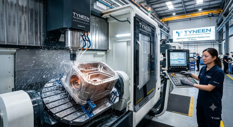
Tyneen delivers turnkey semiconductor chuck engineering and precision ceramic manufacturing. Our facilities integrate multi-axis CNC machining, dedicated cleanroom finishing cells, and advanced sub-micron metrology instrumentation.
Whether you require new prototyping for 300 mm ESC vacuum chucks or serial refurbishment of sintered SiC components, our manufacturing engineers optimize toolpaths, wheel chemistry, and cycle times for yield and longevity.
Connect with our engineering specialists directly to request a tooling quote on your next semiconductor manufacturing project.
Frequently Asked Questions About Wafer Chuck Precision Grinding
What surface flatness tolerances are achievable on 300 mm ceramic chucks?
Using the Tyneen 4S-MCG protocol, 300 mm sintered SiC and AlN chucks achieve global Total Indicated Runout (TIR) under 0.3 µm, with pin-to-pin coplanarity held within ± 0.1 µm across the entire active clamping area.
How do you prevent diamond wheel loading when grinding porous ceramic chucks?
Porous ceramic matrices create abrasive swarf that easily packs diamond wheels. We apply continuous in-process dressing (ELID) alongside high-pressure, directed coolant jets that dynamically evacuate ceramic particles from the wheel matrix.
How many times can an electrostatic chuck (ESC) be re-ground before replacement?
Depending on dielectric layer thickness and the extent of plasma etching erosion, a ceramic ESC substrate can typically undergo 3 to 5 full reconditioning and precision regrinding cycles before critical structural minimums are reached.
How is ductile-mode ceramic grinding verified during production?
We verify ductile-mode grinding non-destructively using non-contact 3D white light interferometry to assess surface texture (Sa, Sq) and cross-polarized optical microscopy to confirm the complete absence of micro-fracturing along pin edges.
Need Sub-Micron Precision on Your Semiconductor Chucks?
Speak directly with Tyneen’s ultra-precision engineering team to review CAD models, ceramic substrate tolerances, and cleanroom manufacturing requirements.