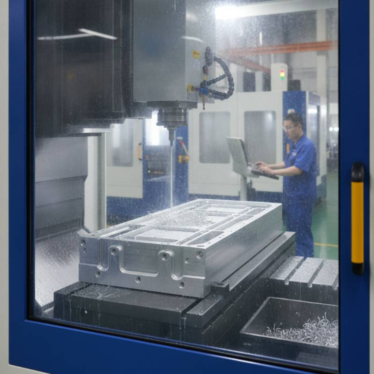
Precision Grinding for Semiconductor Wafer Chucks
Technical Metrology: Achieving Sub-Micron Flatness and TTV
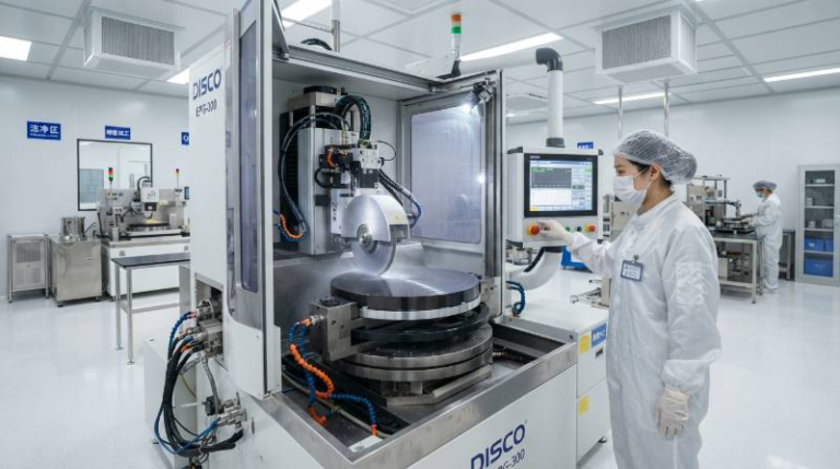
Precision Grinding for Semiconductor Wafer Chucks is the specialized machining process used to achieve extreme surface flatness and parallelism on the components that hold silicon wafers during fabrication. By utilizing diamond-abrasive technology, this process ensures that the chuck surface remains uniform within nanometer tolerances, which is essential for maintaining the focal depth required in advanced lithography.
In 2026, the semiconductor industry has reached a tipping point where traditional lapping no longer meets the stringent requirements of 2nm nodes. Modern wafer fab equipment requires chucks with near-perfect Total Thickness Variation (TTV) to prevent pattern distortion.
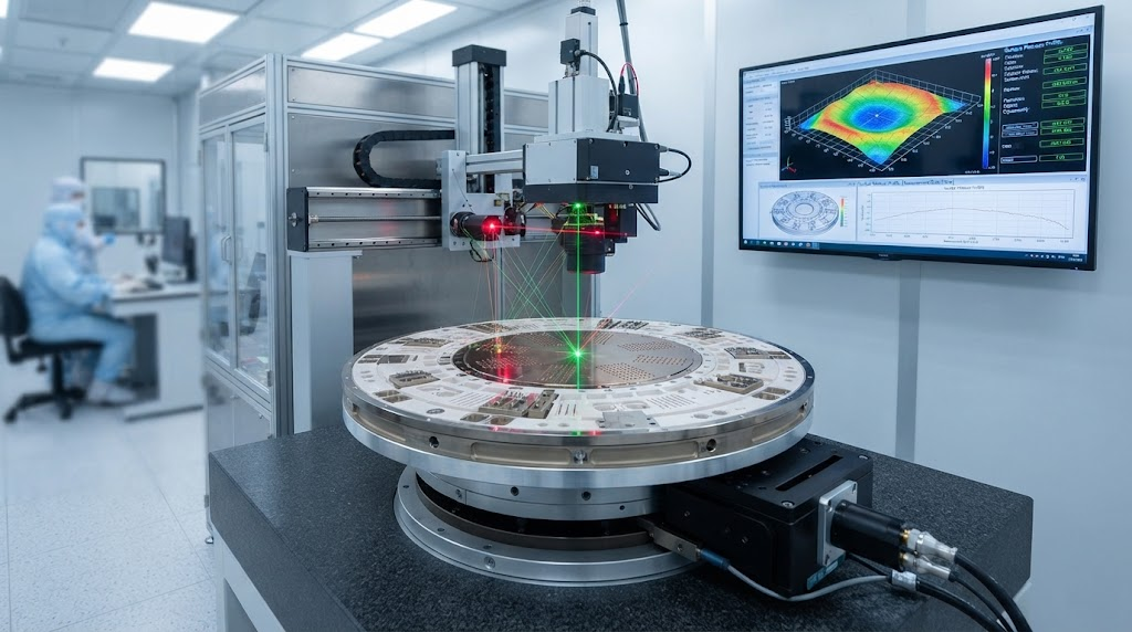
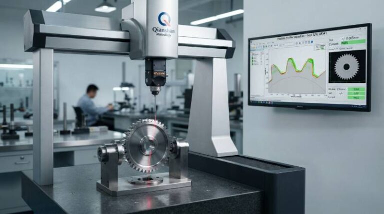
Our data indicates that even a 0.5-micron deviation in flatness can lead to a significant drop in die yield during Extreme Ultraviolet (EUV) exposure. Achieving micron-level accuracy requires in-situ measurement systems that monitor the grinding wheel’s path in real-time.
| Metric | Standard (Legacy) | Advanced (2nm Ready) |
|---|---|---|
| Surface Flatness | < 2.0 µm | < 0.25 µm |
| Total Thickness Variation (TTV) | < 1.5 µm | < 0.15 µm |
| Surface Roughness (Ra) | < 0.1 µm | < 0.01 µm |
Material Science: Grinding Alumina vs. Silicon Carbide (SiC)
The choice between Alumina ceramic and Silicon Carbide (SiC) significantly impacts the grinding strategy. While Alumina remains a staple for many vacuum chucks, SiC has become the preferred material for high-power plasma environments due to its superior thermal stability and stiffness.
Grinding SiC presents unique challenges because of its extreme hardness and brittle nature. We utilize specialized vitrified bond diamond wheels to manage the high heat generated during the process, preventing micro-cracking in the porous ceramic chuck structures.
For high-performance Semiconductor Manufacturing Solutions, the thermal expansion coefficient of the chuck must match the wafer as closely as possible. SiC’s ability to dissipate heat quickly makes it ideal for the rapid thermal cycling found in modern etching processes.
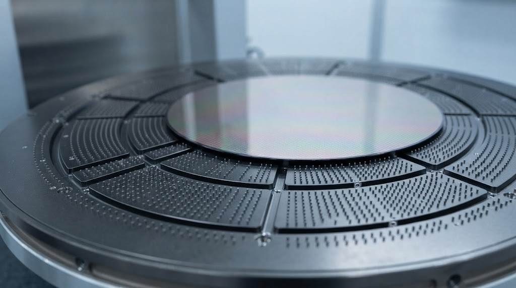
The Nano-Parallel™ Alignment Framework
We have developed a proprietary methodology known as the Nano-Parallel™ Alignment Framework. This 4-step protocol ensures that the grinding spindle and the chuck mounting surface are perfectly synchronized before any material is removed.
- Kinematic Mapping: Measuring the machine’s inherent geometric errors under thermal load.
- Dynamic Balancing: Eliminating spindle vibration that causes “chatter” marks on the ceramic surface.
- Sub-Micron Zeroing: Aligning the diamond wheel to the chuck plane using contact-less sensors.
- Iterative Metrology: Grinding in small increments with mid-cycle inspections to account for material stress relief.
“Achieving sub-micron parallelism isn’t just about the machine; it’s about controlling the environment. At the 2nm node, even the slightest atmospheric pressure change can throw off your metrology.”
— Senior Process Engineer, Microelectronics Division
Impact on EUV Lithography: Yield Rates at 2nm Nodes
In EUV lithography, the depth of focus is incredibly shallow. If an electrostatic chuck (ESC) has even a minor tilt or non-uniformity, the wafer will sit outside the optimal focal plane. This results in “blurring” of the circuit patterns, leading to immediate die failure.
Through our Precision Machining Services, we focus on maximizing the “chuck-to-wafer” contact area. By optimizing surface parallelism, we ensure that the electrostatic clamping force is distributed evenly across the entire 300mm or 450mm surface.
This precision is particularly vital for ASML equipment compatibility. As the industry moves toward 450mm wafer prototypes, the leverage effect of a slightly un-parallel chuck becomes magnified, making our Nano-Parallel™ approach indispensable for future-proofing fab operations.
Sustainability: Reducing Waste in High-Volume Grinding
The environmental footprint of semiconductor manufacturing is under intense scrutiny. High-volume precision grinding typically consumes large amounts of coolant and energy. Our sustainability audit focuses on high-efficiency coolant recycling and optimized grinding cycles that reduce energy consumption by up to 20%.
Instead of discarding worn electrostatic chucks, we recommend a robust program of Equipment Maintenance & Refurbishment. Re-grinding a chuck to restore its flatness is a fraction of the cost of a new unit and saves kilograms of high-purity ceramic material from landfills.
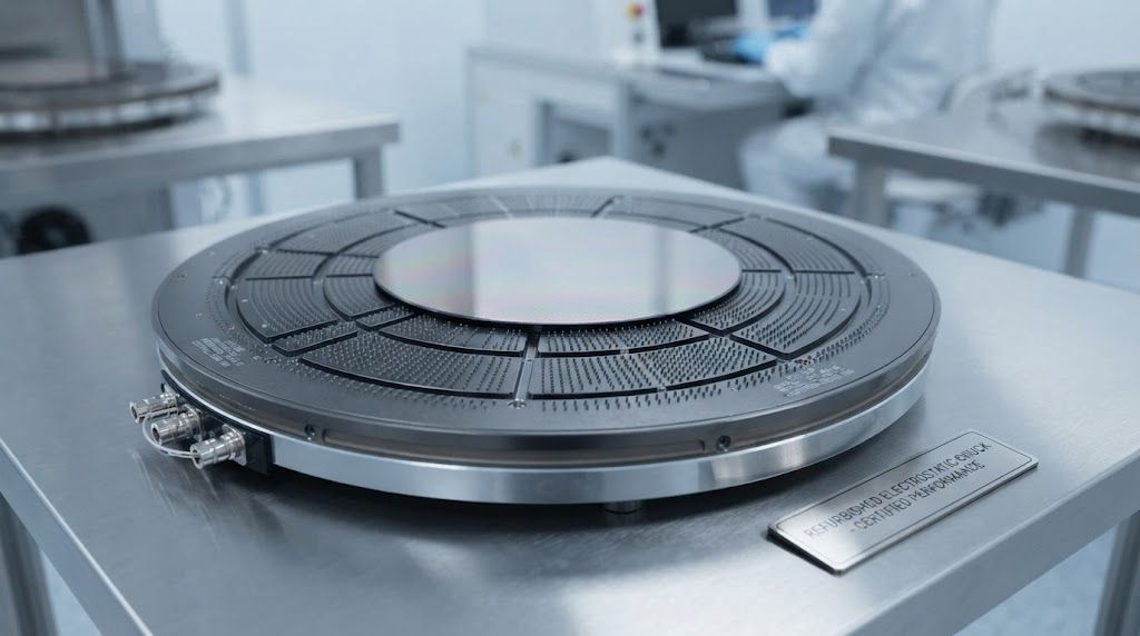
The ROI on refurbishment is clear: a typical ESC can be refurbished 3-5 times before reaching its minimum thickness threshold. This extends the lifecycle of critical wafer fab equipment while maintaining the sub-micron accuracy required for 2026 production standards.
Frequently Asked Questions
What is the difference between grinding and lapping for wafer chucks?
Grinding is a fixed-abrasive process that offers higher geometric control and faster material removal. Lapping uses loose abrasives and is generally slower and less precise for maintaining specific parallelism across large diameters like 300mm wafers.
How often should an electrostatic chuck be re-ground?
Frequency depends on the plasma environment and the chemicals used in etching. Typically, an inspection is recommended every 5,000 to 10,000 wafer cycles to check for surface erosion or loss of clamping force.
Why is Silicon Carbide (SiC) harder to grind than Alumina?
SiC has a much higher hardness rating (9.5 on the Mohs scale), which requires specialized diamond wheels and very specific feed rates to avoid inducing surface stress or thermal damage during the machining process.
Expert Review and Industry References
This technical guide was reviewed by our Lead Metrology Specialist, who brings over 15 years of experience in microelectronics fabrication and precision machining. Our methodologies align with the latest SEMI industry standards for wafer handling and equipment specifications.
- SEMI Standards: Semiconductor Equipment and Materials International
- IEEE Xplore: Advanced Lithography and Metrology Research
Ready to Optimize Your Wafer Yield?
Ensure your fab equipment meets the 2nm challenge with our sub-micron grinding expertise.