Ultra-Precision CNC Milling for Semiconductor Equipment
Ultra-Precision CNC Milling for Semiconductor Equipment
What is Ultra-Precision CNC Machining for Semiconductors?
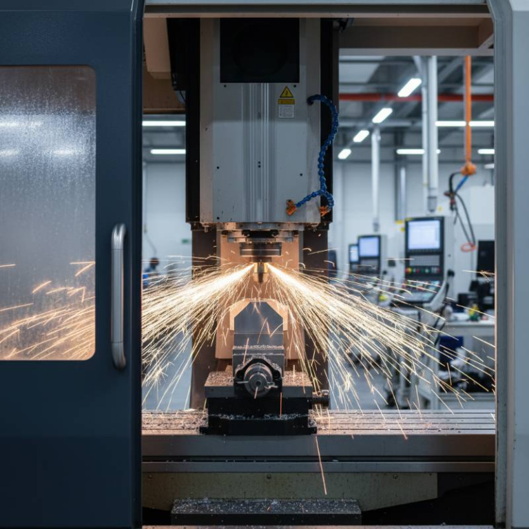
Ultra-precision CNC milling for semiconductor equipment is a specialized manufacturing process designed to produce components with sub-micron accuracy and exceptional surface integrity. This discipline is essential for creating the complex geometries found in gas delivery systems, wafer chucks, and thermal management modules.
In 2026, as chip architectures shrink below 2nm, the demand for Precision Engineering Services has reached a critical peak. We define this level of machining not just by dimensional accuracy, but by the total elimination of microscopic defects that could lead to particle generation or outgassing in a vacuum environment.
Engineering for Ultra-High Vacuum (UHV) Compatibility
Achieving Ultra-High Vacuum (UHV) environments—often exceeding 10^-9 Torr—requires more than just a smooth finish. It demands a fundamental shift in how we approach semiconductor CNC machining.
Outgassing Prevention Machining: A specialized manufacturing methodology that eliminates trapped air pockets and surface contaminants to ensure rapid vacuum draw-down and long-term pressure stability.
Our approach to Vacuum Chamber Manufacturing focuses on several critical design features:
- No Blind-Hole Designs: Every threaded hole is either through-drilled or equipped with venting channels to prevent “virtual leaks.”
- Precision O-Ring Grooves: We machine seal surfaces to a mirror finish, ensuring zero-leak interfaces for elastomer or metal seals.
- Venting Grooves: Strategic pathways are integrated into nested components to allow gas to escape during pump-down cycles.
The PurePath™ 5-Step Precision Protocol
To maintain absolute consistency across global supply chains, we have pioneered the PurePath™ Protocol. This proprietary framework ensures every component meets the rigorous demands of Tier-1 semiconductor OEMs.
- Material Stabilization: Cryogenic stress-relieving of alloys to prevent dimensional “creep” after machining.
- Thermal-Compensated Milling: Real-time adjustment of spindle and tool paths based on ambient temperature fluctuations in the facility.
- Ultrasonic Deburring: Using high-frequency cavitation to remove microscopic burrs that traditional mechanical methods miss, ensuring zero particle shedding.
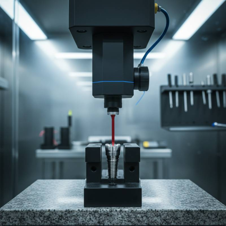
- SEMI-Standard Inspection: Multi-axis CMM verification mapped against SEMI standards for geometric dimensioning and tolerancing (GD&T).
- Hermetic Cleanroom Packaging: Final assembly in Class 100 environments followed by double-layer vacuum sealing.

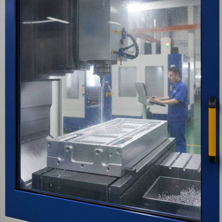
Technical Specifications: Tolerances and Surface Integrity
Precision in the semiconductor world is measured in microns. Our milling centers are calibrated to exceed standard industry outputs, providing the following benchmarks for complex 6061-T651 aluminum and ceramic parts.
| Parameter | Standard Precision | Tyneen Ultra-Precision |
|---|---|---|
| Dimensional Tolerance | ±0.010 mm | ±0.002 mm |
| Surface Roughness (Ra) | 0.8 μm | 0.2 μm |
| Vacuum Capability | 10^-6 Torr | <10^-9 Torr (UHV) |
| Particle Control | Standard Wash | Ultrasonic + ISO Class 4 |
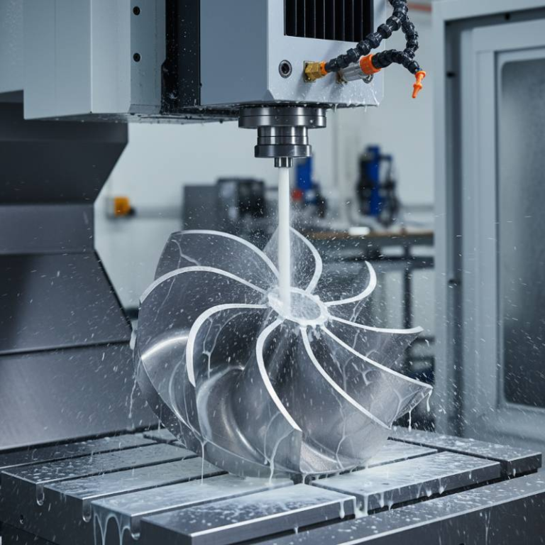
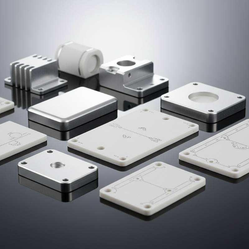
Material Excellence: High-Purity Aluminum and Ceramics
The choice of material dictates the longevity of the equipment in corrosive plasma environments. We specialize in Advanced Material Solutions, focusing on alloys that exhibit minimal outgassing and high thermal conductivity.
High-Purity Aluminum 6061-T651: This remains the industry workhorse. However, our 2026 processing techniques involve specialized anodization-ready surfaces that prevent cracking under thermal cycling. We’ve published a comprehensive Technical White Paper on High-Purity Aluminum Machining specifically for Tier-1 process engineers.
Beyond metals, our expertise extends to specialty ceramics and high-performance polymers like PEEK, which are crucial for wafer handling where metallic contamination must be strictly avoided.
SEMI Compliance and Cleanroom Assembly Standards
Manufacturing the part is only half the battle. Preventing contamination during the “last mile” is where many suppliers fail. Our facility operates ISO Class 4 and 5 cleanrooms for final inspection and assembly.
Adhering to SEMI standards ensures that our components integrate seamlessly into larger lithography or etching tools. Our double-layer vacuum packaging process involves purging the inner layer with high-purity nitrogen, providing a moisture-free environment that preserves the Ra 0.2μm surface finish until the moment of installation.
Sustainability and Real-Time Telemetry in CNC Milling
The semiconductor industry is under increasing pressure to reduce its carbon footprint. At Tyneen, we have integrated real-time floor telemetry into our milling centers. This allows us to monitor spindle-time efficiency and energy consumption per part.
By optimizing tool paths through AI-driven CAM software, we reduce material waste by up to 15% compared to traditional milling methods. This data is available to our partners as part of their ESG reporting requirements, ensuring that high-performance machining doesn’t come at an environmental cost.
Frequently Asked Questions
How do you verify helium leak rates for vacuum chambers?
Every chamber undergoes helium mass spectrometer leak testing. We guarantee leak rates lower than 1×10^-9 mbar·L/s, ensuring long-term stability in UHV environments.
What is the typical lead time for complex CNC semiconductor parts?
While complexity varies, our streamlined PurePath™ process typically delivers prototypes in 2-3 weeks and production batches in 6-8 weeks, depending on material availability.
Do you provide material certifications for 6061-T651?
Yes. All materials are sourced from Tier-1 mills and come with full chemical and physical property certifications, including traceability back to the original melt lot.
Ready to Scale Your Semiconductor Production?
Download our Technical White Paper on High-Purity Aluminum Machining or request a 24-hour quote for your precision components.